A Digispark ATtiny85 development board is a microcontroller board with an ATtiny85 MCU chip. It is a favorite board for projects that require a small number of GPIOs. The board is basically an ATtiny85 chip that is provided with a voltage regulator and a USB interface. We will take a look at the Digispark ATtiny85 pinout and the different configurations that it has to offer.
Types of Digispark Boards
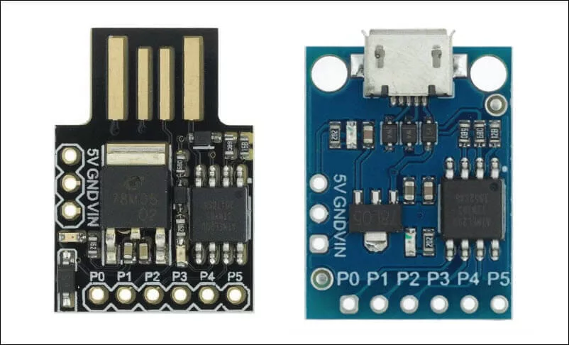
Figure 1 shows the two (2) popular versions of the Digispark ATtiny85 development boards. The one on the left uses a type-A USB connector to connect directly to the USB port of a PC or a laptop. On the other hand, the board on the right has a micro-USB connector. As a result, we need a micro-USB cable to connect this to a computer for programming purposes.
It should be observed that both boards have the same pin layout. We can breadboard them as long as we do not connect a header pin to the VIN terminal.
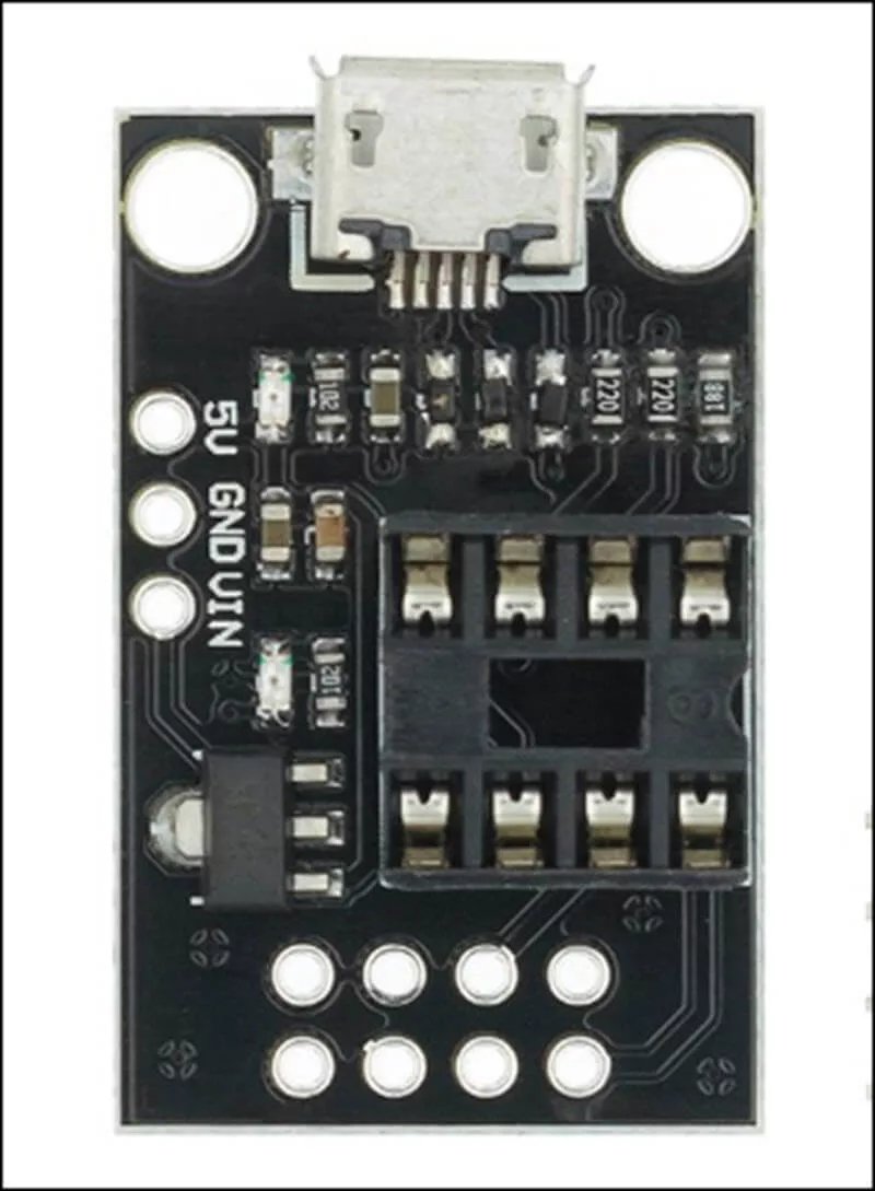
Figure 2 is a picture of another type of Digispark ATtiny85 board. As shown in the picture, the board does not have an ATtiny85 chip but instead only an 8-pin DIP socket. We must provide a DIP-type ATtiny85 chip in order to use this board. Also, the pin layout of this board is different. This board is not breadboard friendly. However, the pin layout is ICSP-programmer ready. That is, the pins are arranged so as to accept the female connector of an AVR ICSP-programmer.
It must be mentioned here that technically, this board is not (yet) a Digispark ATtiny85 board. A Digispark ATtiny85 board has an ATtiny85 chip that was burned with a Micronucleus bootloader. In order to make this board a Digispark board, it needs an ATtiny85 chip that was pre-programmed with a Micronucleus bootloader. Otherwise, an ATtiny85 without a bootloader can be inserted into the DIP socket and an ICSP programmer is used to burn a new Micronucleus bootloader into it.
Digispark ATtiny85 Specifications
- Support for the Arduino IDE 1.0+ (OSX/Win/Linux)
- Power via USB or External Source – 5v or 7-35v (12v or less recommended, automatic selection)
- On-board 500ma 5V Regulator
- Built-in USB
- 6 I/O Pins (2 are used for USB only if your program actively communicates over USB, otherwise you can use all 6 even if you are programming via USB)
- 8k Flash Memory (about 6k after bootloader)
- I2C and SPI (vis USI)
- PWM on 3 pins (more possible with Software PWM)
- ADC on 4 pins
- Power LED and Test/Status LED
Digispark ATtiny85 Pinout
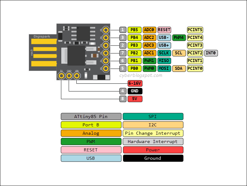
Digispark ATtiny85 Pinout Description
ATtiny85 Breakout
First of all, by referring to Figure 3, you will notice that the Digispark board serves as a breakout board for the ATtiny85 chip. All of the eight pins of the ATtiny85 chip are accessible. The physical pins of the ATtiny5 chip are designated by the gray-colored pinouts numbered 1 to 8.
Six (6) Digital I/O Pins
As per specification, the Digispark ATtiny85 board can be configured to use six (6) digital I/O ports. These ports are shown in Figure 3 as yellow pins, labeled PB0 to PB5. NOTE: Port B pin PB5 is by default configured as a RESET pin. In order to use PB5 as an I/O port, an ATtiny85 fuse (RSTDISBL) has to be reset (changed from 1 to 0). Please see How to Reset ATtiny85 Fuses.
Arduino IDE Programming Notes
In the Arduino IDE, pins PB0 to PB5, when used as digital I/O are referred to as 0 to 5. That is,
/*
cyberblogspot.com 09Jan2023
*/

bool a, b, c;

void setup() {
  // put your setup code here, to run once:
  pinMode(0, INPUT);   //set PB0 as input
  pinMode(1, INPUT);   //set PB1 as input
  pinMode(2, INPUT);   //set PB2 as input
  pinMode(3, OUTPUT);  //set PB3 as output
  pinMode(4, OUTPUT);  //set PB4 as output
  pinMode(5, OUTPUT);  //set PB5 as output
}

void loop() {
  // put your main code here, to run repeatedly:
  a = digitalRead(0);     //read PB0
  b = digitalRead(1);     //read PB1
  c = digitalRead(2);     //read PB2
  digitalWrite(3, LOW);   //set PB3 LOW
  digitalWrite(4, LOW);   //set PB4 LOW
  digitalWrite(5, HIGH);  //set PB5 HIGH
}
Four (4) Analog to Digital Converter (ADC) Ports
Port B ports PB2 to PB5 can be configured as analog inputs. These pins are shown in Figure 3 as orange pins. The pins are labeled ADC0 to ADC3. Be aware that the Port B numbers do not exactly match the ADC port numbers. In other words, PB2 does not correspond ADC2, PB3 does not correspond to ADC3, and so on. Instead,
- ADC0 is PB5
- ADC1 is PB2
- ADC2 is PB4
- ADC3 is PB3
Arduino IDE Programming Notes
When using the command analogRead(), Arduino IDE assumes you are using the ADC port numbers (0 for ADC0, 1 for ADC1, 2 for ADC2, and 3 for ADC3) and NOT the Port B numbers (0 for PB0, 1 for PB1, 2 for PB2, 3 for PB3, 4 for PB4, and 5 for PB5). However, the pinMode() command expects you to use the Port B numbers. This is one of ATtiny85’s peculiarities that is very confusing. The example code below should clear this up.
/*
cyberblogspot.com 09Jan2023
*/

int a, b, c, d;

void setup() {
// put your setup code here, to run once:
// the following four lines of code are actually not needed
// because by default the I/O pins are in Hi-Z INPUT mode
pinMode(2, INPUT); //set PB2 as input
pinMode(3, INPUT); //set PB3 as input
pinMode(4, INPUT); //set PB4 as input
pinMode(5, INPUT); //set PB5 as input
}

void loop() {
// put your main code here, to run repeatedly:
a = analogRead(0); //read ADC0 which is in PB5
b = analogRead(1); //read ADC1 which is in PB2
c = analogRead(2); //read ADC2 which is in PB4
d = analogRead(3); //read ADC3 which is in PB3
}
Three (3) Pulse Width Modulation (PWM) Outputs
Referring again to Figure 3, there are three (3) PWM outputs available on Digispark ATtiny85 boards. These are colored green in the pinout shown above and are labeled as PWM0, PWM1, and PWM4. There is no typo error here. The third PWM output is labeled as PWM4 because the PWM port numbers use the same Port B numbers. To clarify,
- PWM0 is PB0
- PWM1 is PB1
- PWM4 is PB4
Arduino IDE Programming Notes
The PWM output signal is generated by the command analogWrite(). Although we are going to use the ports as analog outputs, we DO NOT use the ADC port numbers. Rather, we use the PWM port numbers which are the same as the Port B numbers. In other words, we are also using the Port B numbers in programming PWM in the Arduino IDE. Please take a look at the following sketch.
/*
cyberblogspot.com 09Jan2023
*/

void setup() {
  // put your setup code here, to run once:
  pinMode(0, OUTPUT);  //set PB0 (PWM0) as output
  pinMode(1, OUTPUT;  //set PB1 (PWM1) as output
  pinMode(4, OUTPUT);  //set PB4 (PWM4) as output
}

void loop() {
  // put your main code here, to run repeatedly:
  analogWrite(0, 255);  //100% duty cycle PWM on PB0
  analogWrite(1, 128);  //50% duty cycle PWM on PB1
  analogWrite(4, 0);    //0% duty cycle PWM on PB4
}
SPI (Serial Peripheral Interface) Communication
Ports PB0, PB1, and PB2 can be used for SPI communication:
- MOSI – PB0
- MISO – PB1
- SCLK – PB2
I2C (Inter-Integrated Circuit) Communication
Ports PB0 and PB2 can be used for I2C communication:
- SDA – PB0
- SCK – PB2
USB (Universal Serial Bus) Communication
Ports PB3 and PB4 can be used for USB communication:
- USB- is PB4
- USB+ is PB3
Pin Change Interrupt and External Interrupt
Finally, ports PB0 to PB5 can all be used for pin change interrupt and PB2 as external interrupt pin.
Final Notes on Port B Pins
PB5 has limited current sourcing capacity. Also, when it is at output HIGH, it generates 3V instead of 5V on its output.
PB3 and PB4 are both used during programming (sketch upload). Therefore, it may be necessary to temporarily disconnect the circuits connected to them to avoid interfering with the uploading of sketches. Additionally, PB3 has a 1.5K pull-up resistor that is used for USB communication.
PB0 or PB1 has the built-in LED attached to it. Version A boards use PB1 while version B boards use PB0.
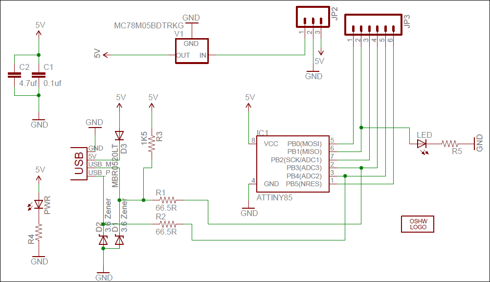
Digispark ATtiny85 Schematic Diagram
References on Digispark ATtiny85 Pinout and Configuration
http://digistump.com/wiki/digispark
ATtiny85 External and Pin Change Interrupt
How to Install Arduino IDE on Windows 10
How to Install ATTinyCore on Arduino IDE
How to Program ATtiny85 with Arduino IDE
How to Program Digispark ATtiny85 Board with Arduino IDE
Digispark USB Device Not Recognized
How to Use AT-09 BLE with Arduino and Smartphone
How do I connect an external USB jack to a DJSpark?
I love these little chips, I tend to use them a lot in my model making where ssce can be tight. Once you get used to them they are so useful.
Hey, thanks for the nice compilation! – digistump.com’s webSite is a little slow?
For _me_ it seems, you reused an image of “Erik Kettenburg, Digistump LLC, digistump.com, 2012” as “digispark-schematic.png”, don’t you? (it would be nice to cite the original source as reference and for credits, don’t you think?)
* If you power the stump via USB only, the 5V for the chip MUST come from USB => ergo D3 must be a schottky (other symbol; must be the “fat one” between PwrLED and P0?) and point into reverse direction?! (I am not sure, if digistump did that black-hearted (-minded), cause it makes no real difference, but for the board fakers, they are annoyed of) – the symbol of the zeners is also wrong – but who cares 😉
* If you power the stump externally (Vin to MC78M05 to 5V Vcc) that diode MUST protect from reverse powering the computer (feeding power back, i.e. wrong way, into a power source)
* I think the 5V pin of (VIN|GND|5V) is only(!) designed as output, to power additional circuits, we plug the stump into?
BRs Klaus
_______
PS: still working on an idea for a second analog read input (for voltage level, not just resistor-ladder/poti, in additon to PB2/A1), but keeping the USB(!) for dia-log-ging… (so only PB5/A0 overload possible?)